[an error occurred while processing this directive]
[an error occurred while processing this directive]
 [an error occurred while processing this directive]
Postdoctoral Researcher
[an error occurred while processing this directive]
University of California, Santa Barbara
[an error occurred while processing this directive]
PhD '19 The Ohio State University
[an error occurred while processing this directive]
[an error occurred while processing this directive]
[an error occurred while processing this directive]
[an error occurred while processing this directive]
[an error occurred while processing this directive]
Postdoctoral Researcher
[an error occurred while processing this directive]
University of California, Santa Barbara
[an error occurred while processing this directive]
PhD '19 The Ohio State University
[an error occurred while processing this directive]
[an error occurred while processing this directive]
[an error occurred while processing this directive]
Energy
Physical Electronics
[an error occurred while processing this directive]
β-Ga₂O₃ and GaN: for Next Generation Energy Efficient High-Power Devices
[an error occurred while processing this directive]
To address the long-standing issues of fossil fuels and climate changes, current high-power technology is actively seeking energy-efficient electronics. The new generation of power devices, with scalable and lightweight designs, are envisioned to support both energy efficiency and environmental security through their integration in future smart energy grids, electric vehicles, satellites as well as many consumer electronics. At the core of power electronics, the wide-bandgap (WBG) and ultrawide bandgap (UWBG) semiconductors serve as the building blocks to facilitate compact and low-loss high-power devices owing to their wide bandgap. However, these materials still have challenges related to their high-quality growth, defect engineering, device processing, harsh environment tolerance, and thermal management that act as bottlenecks to their predicted performances. My research aims to design high-performance vertical devices from the emerging WBG and UWBG semiconductors using advanced field management strategies that enable high breakdown voltage and low on-resistance for efficient switching operations. I have demonstrated GaN-on-GaN p-n diodes from ammonia molecular beam epitaxy that revealed a breakdown voltage over one kilovolt and an ultra-low on resistance, both achieved with a much thinner drift layer compared to the state-of-the-art reports. My works also offered a foundation for high-quality β-Ga₂O₃ Schottky diodes with a possibility of barrier height modulation that will be promising for gate metal engineering of future power devices.
[an error occurred while processing this directive]
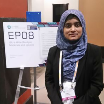
Esmat Farzana is a Postdoctoral Researcher in Materials Department at the University of California, Santa Barbara, working with Prof. James S. Speck. She received her PhD in Electrical Engineering from The Ohio State University in 2019 and Bachelor’s degree from Bangladesh University of Engineering and Technology in 2011. Her research interest lies at the intersection of electrical engineering and materials science with a focus on developing high-power devices using wide bandgap semiconductors, particularly β-Ga₂O₃ and III-nitrides. Her research area also includes investigation of defects and reliability of wide bandgap semiconductors. Her works have been featured as Editor’s pick in Applied Physics Letters and listed among the most cited articles in 2019 in Journal of Applied Physics. In 2019, she was invited by American Institute of Physics (AIP) to be an editor for a book on β-Ga₂O₃ material and devices. Esmat also served as a Lecturer in the Department of Electrical & Electronic Engineering at Ahsanullah University of Science and Technology, Bangladesh prior to joining her PhD in USA in 2013.
[an error occurred while processing this directive]
Personal home page
[an error occurred while processing this directive]
[an error occurred while processing this directive]
 [an error occurred while processing this directive]
Postdoctoral Researcher
[an error occurred while processing this directive]
University of California, Santa Barbara
[an error occurred while processing this directive]
PhD '19 The Ohio State University
[an error occurred while processing this directive]
[an error occurred while processing this directive]
[an error occurred while processing this directive]
[an error occurred while processing this directive]
[an error occurred while processing this directive]
Postdoctoral Researcher
[an error occurred while processing this directive]
University of California, Santa Barbara
[an error occurred while processing this directive]
PhD '19 The Ohio State University
[an error occurred while processing this directive]
[an error occurred while processing this directive]
[an error occurred while processing this directive]